Intro
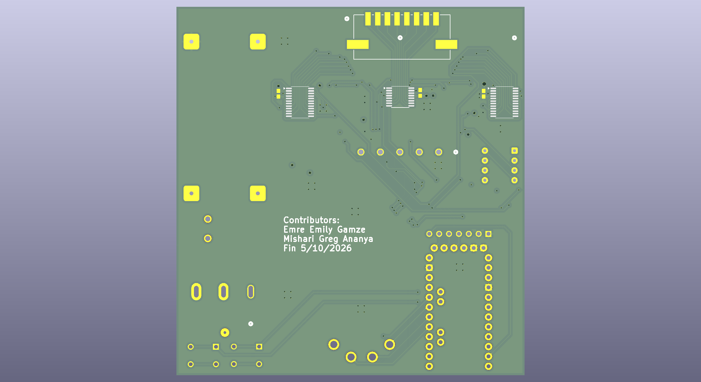
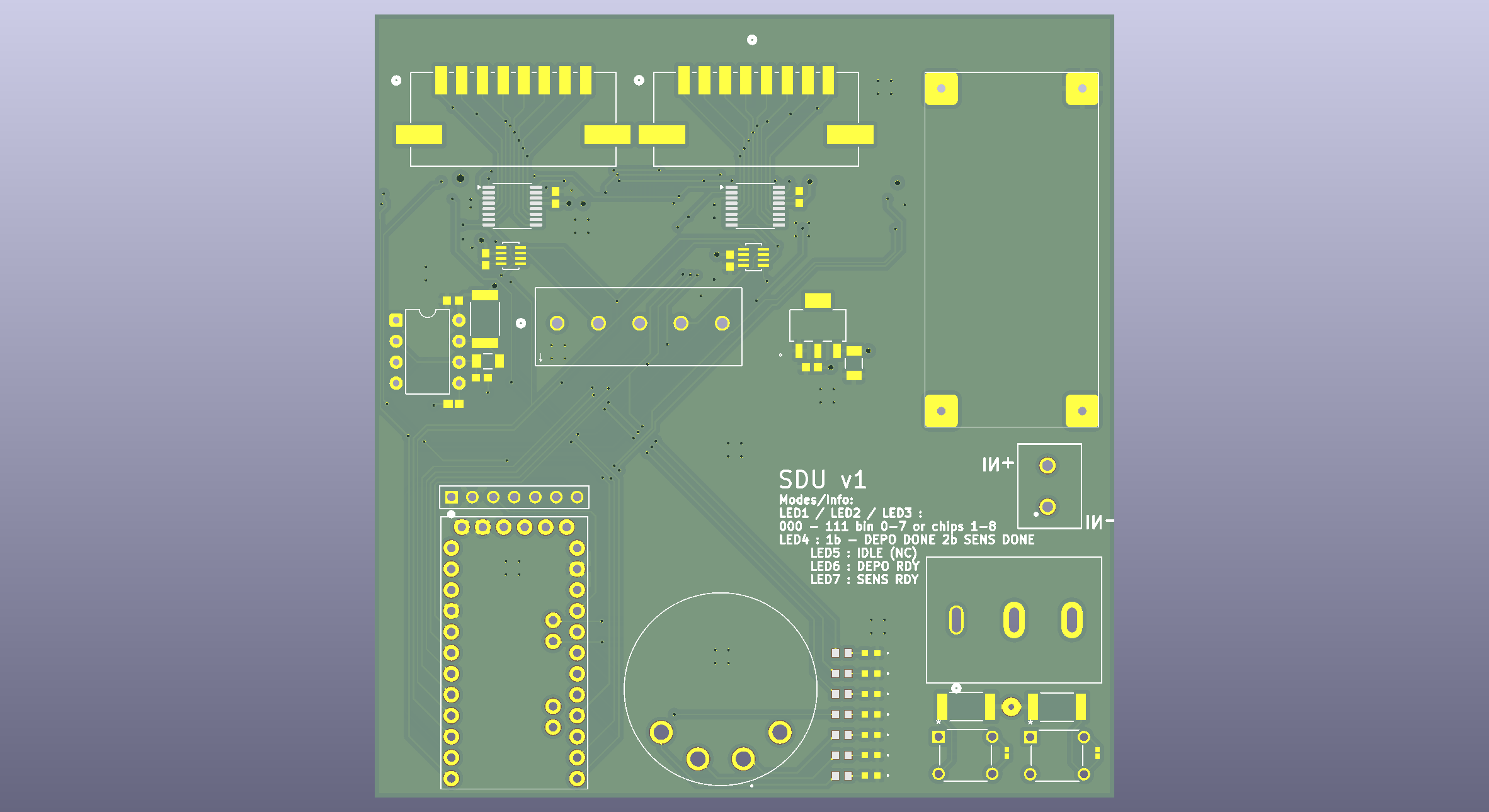
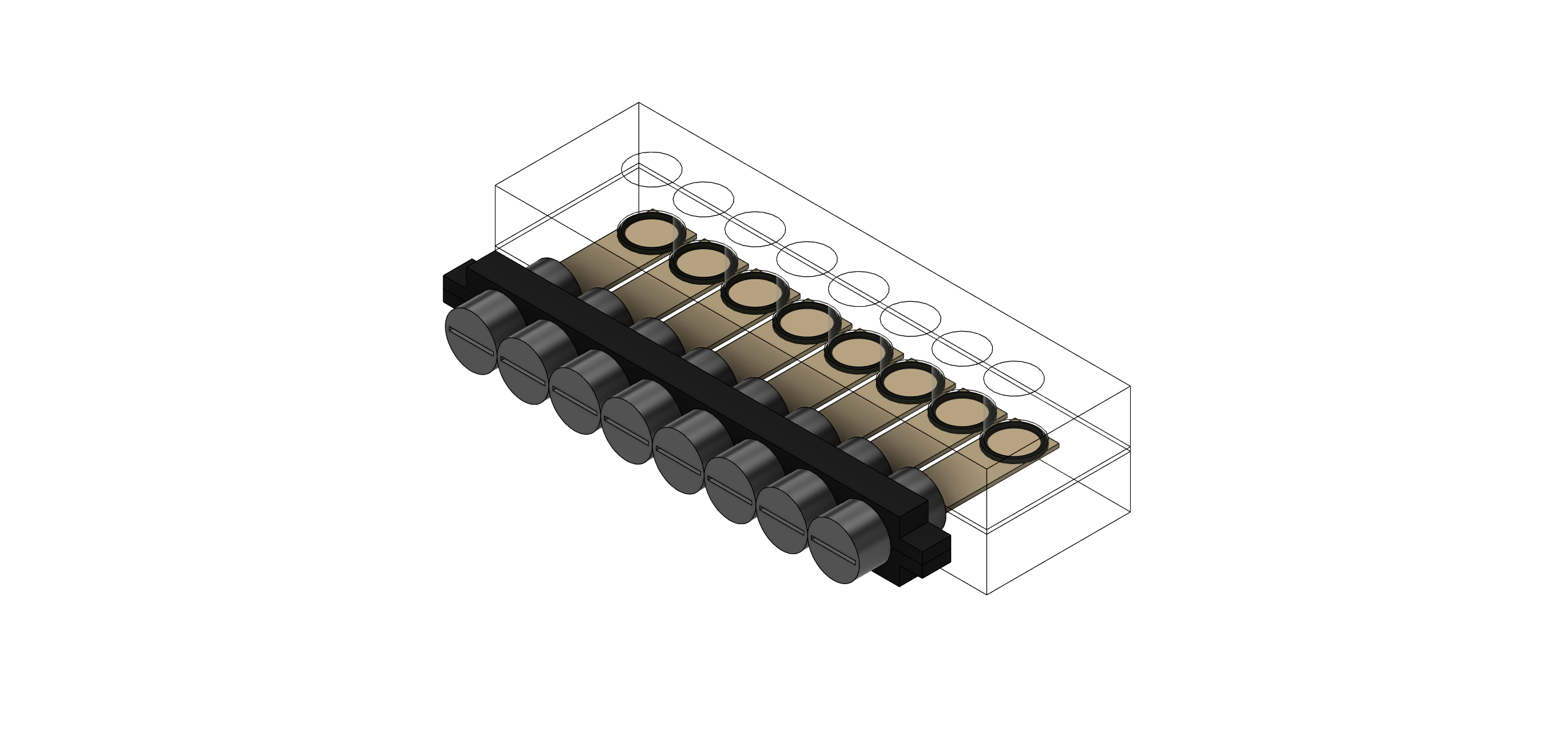
The Sensor Deposition Unit is an attachable electrical subsystem for Terry/ASATS, a lower-cost IsoPure-style magnetic bead agitation platform used in the lab. Terry/ASATS handles the bead-processing side of the workflow. The SDU adds the electrical layer: controlled deposition and electrochemical sensing across multiple biosensor chips.
The project is active. The board and parts have been ordered, and the next stage is soldering, bring-up, and comparison against baseline EmStat Pico measurements.
Purpose
The unit routes deposition and sensing signals across multiple BVT chips while preventing signal paths from touching when they should not. Deposition and sensing are part of the same workflow, but electrically they ask for very different behavior.
During deposition, the system drives a square-wave signal across the chips. During sensing, the EmStat Pico needs a clean electrochemical path for cyclic voltammetry and square-wave voltammetry. That difference is why signal clarity and isolation are the priority. A useful sensing result depends on knowing that the potentiostat is measuring the selected chip, not a path accidentally influenced by the deposition circuit, a neighboring electrode, or a wet mechanical leak.
System context
- Terry/ASATS: lab magnetic bead agitation and processing platform
- Sensor Deposition Unit: attachable electrical subsystem
- BVT chips with three electrode contacts per chip
- More than 24 electrode connections across the full system
- EmStat Pico for electrochemical readout
- 555-timer deposition path for the deposition signal
- Arduino Pro Mini at 8 MHz / 3.3 V for local control
- Simple board-side controls and a single external handoff signal from Terry/ASATS
Operating modes
Deposition Mode
- 10 Vpp square wave at 50 Hz
- Applied to all chips simultaneously
- Generated through a 555-based deposition path
Sensing Mode
- EmStat Pico potentiostat
- Cyclic voltammetry and square-wave voltammetry support
- One chip selected at a time
- Switching isolation protects sensing electronics from deposition drive
Implementation
The architecture separates deposition from sensing. In deposition mode, the 555-based signal path is routed to the chips together. In sensing mode, the deposition path is disconnected and the EmStat Pico is routed to one chip at a time.
That multiplexing choice is the central design tradeoff. It reduces hardware count and keeps a validated potentiostat in the workflow, but it pushes difficulty into relay or switch selection, channel isolation, state timing, and validation. The board has to prove that the selected electrode path is the only meaningful path.
The system behaves like a small state machine. It has to know which mode is active, which path is allowed to connect, and when a signal is safe to pass through. No deposition and sensing path should fight the other.
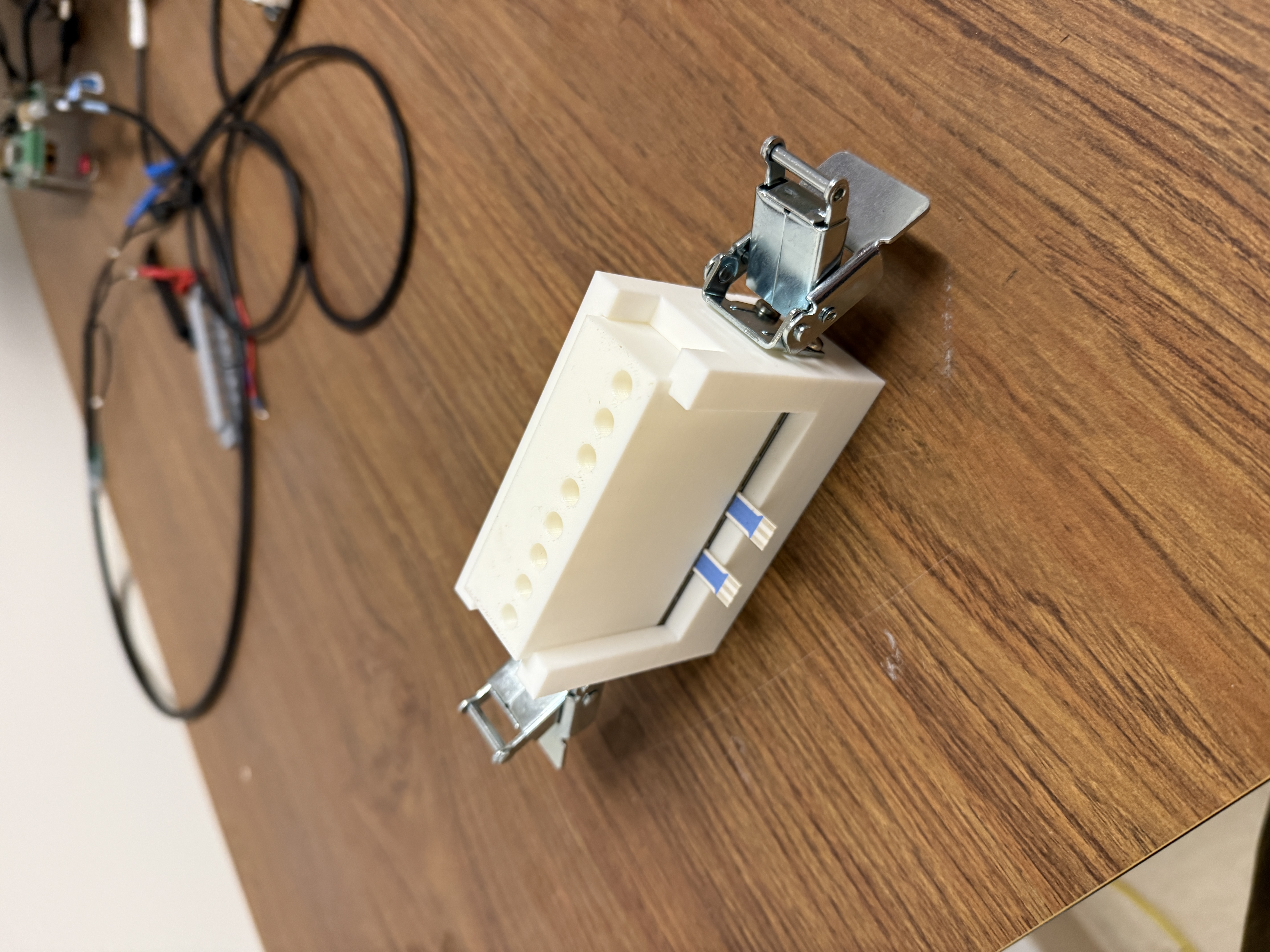
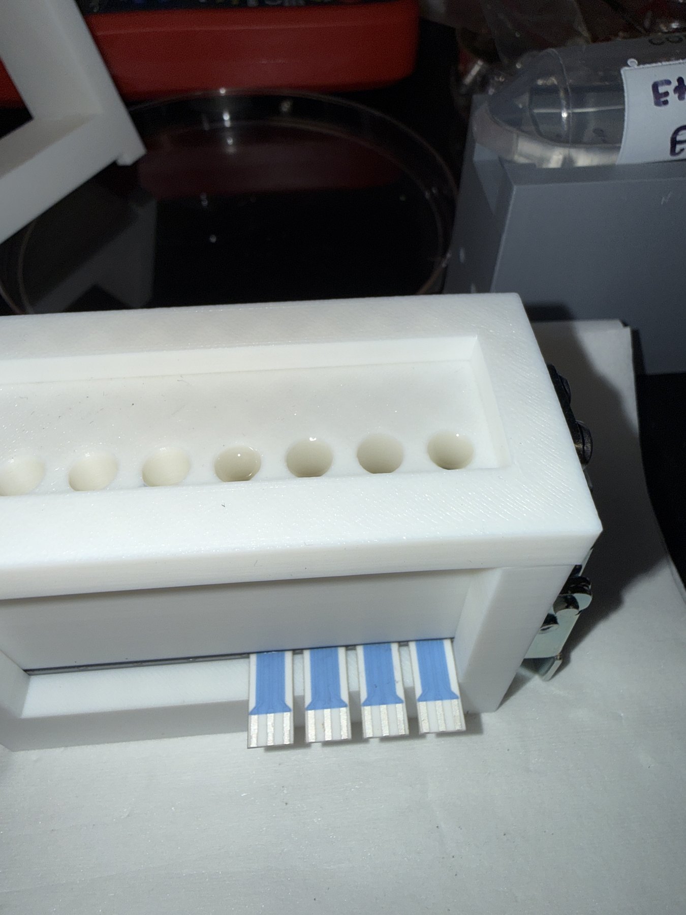
The manifold work is just as important as the PCB. The fixture must apply enough pressure to seal a single silicone gasket, hold BVT chips and their contacts consistently, and sit beside the magnetic bead agitation process without making the workflow harder.
Design decisions
| Decision | Selected direction | Why it fits the system | Tradeoff / next step |
|---|
| Control interface | Board-side controls | Keeps the subsystem focused on reliable mode selection and lab use | Less flexible than a full software interface |
| Sensing | EmStat Pico routed to one chip at a time | Preserves trusted potentiostat behavior while adding multiplexing | Sequential readout limits simultaneous sensing |
| Deposition | Shared 555-based deposition path | Applies the deposition condition across chips together | Isolation must be proven before full workflow use |
| Controller | Arduino Pro Mini, 8 MHz / 3.3 V | Small, familiar, and enough for state and switching control | Not the final answer if UI or logging grows |
| Integration | Single handoff signal from Terry/ASATS | Simple boundary between magnetic processing and electrochemical sensing | More automation can be layered on after bring-up |
Current status
The PCB and parts have been ordered. The next steps are assembly, board bring-up, and validation.
Planned validation sequence:
- Solder and inspect the board
- Confirm board power rails
- Verify switching logic and mode transitions
- Compare EmStat Pico one-plex baseline against the SDU-routed path
- Confirm signals do not interact across channels
- Verify deposition routing across all chips
- Validate one-chip sensing before full multi-chip operation
- Integrate with Terry/ASATS after subsystem validation
Results so far
- System architecture defined
- Board and parts ordered
- Deposition and sensing modes specified
- EmStat Pico sensing path selected
- Manifold and leakage test fixtures modeled
- Integration target defined through Terry/ASATS signal handoff
Future work
- Assemble and bring up the ordered board
- Validate isolation behavior
- Compare EmStat Pico measurements before and after SDU routing
- Refine the manifold and gasket pressure structure
- Automate sequential sensing across chips
- Explore longer-term full workflow automation, including solution movement